Summary
Our team won the EECS151/251A Outstanding Designer Award for the Fall 2022 semester.
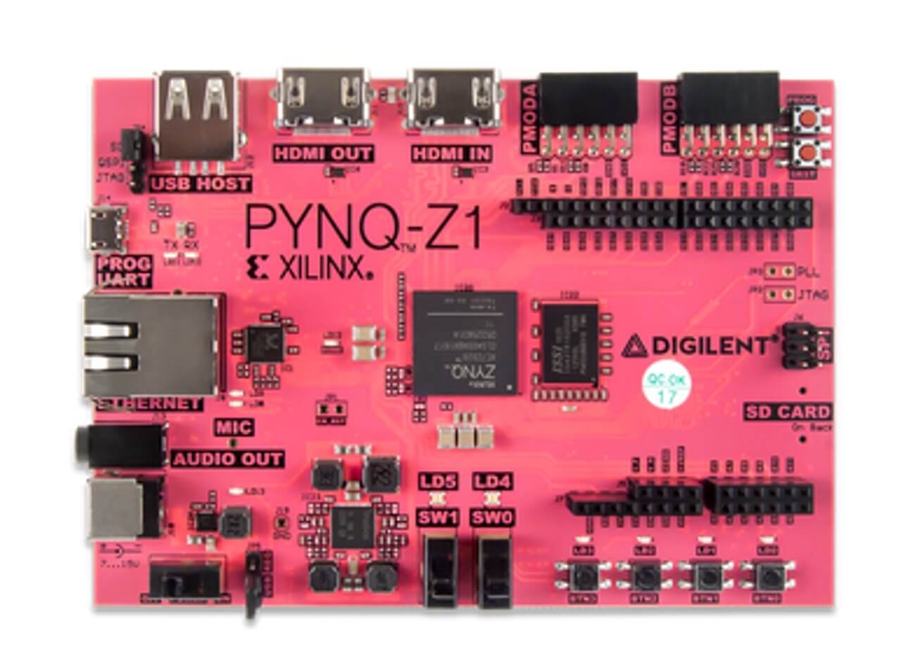
The CPU is implemented using Verilog, targeting the Xilinx PYNQ platform (a PYNQ-Z1 development board with a Zynq 7000-series FPGA). Supports the entire RISC-V ISA. The CPU is able to be receive compiled RISC- V binaries though the UART, store them into instruction memory, then jump to the downloaded program.
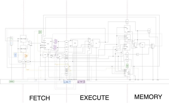
The three stages of the pipeline are:
1. Fetch: An instruction is fetched from the instruction memory or BIOS memory and decoded, then the relevant data is retrieved from the regfile or immediate generator.
2. Execute: The instruction is executed.
3. Memory: There is BIOS memory, instruction memory, data memory and I/O, which we read/write to accordingly and then the final output is committed (written back).
Memory Mapped I/O
We utilized the UART protocol to accomplish the low-level task of sending and receiving bits from the serial lines, and use something called memory-mapped I/O to allow the CPU to send and receive bytes to and from the UART.
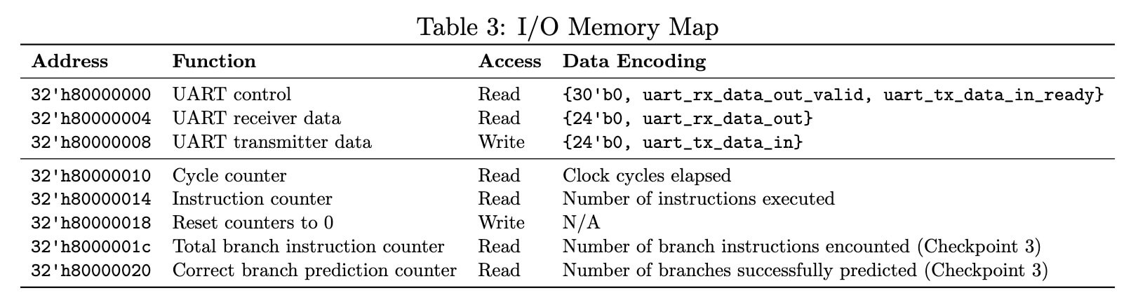
Registers of I/O devices are assigned specific memory addresses, which enables load/store instructions to access them as if they were memory. This memory map is translated into the proper ready-valid handshake signals for the UART.
Branch Predictor
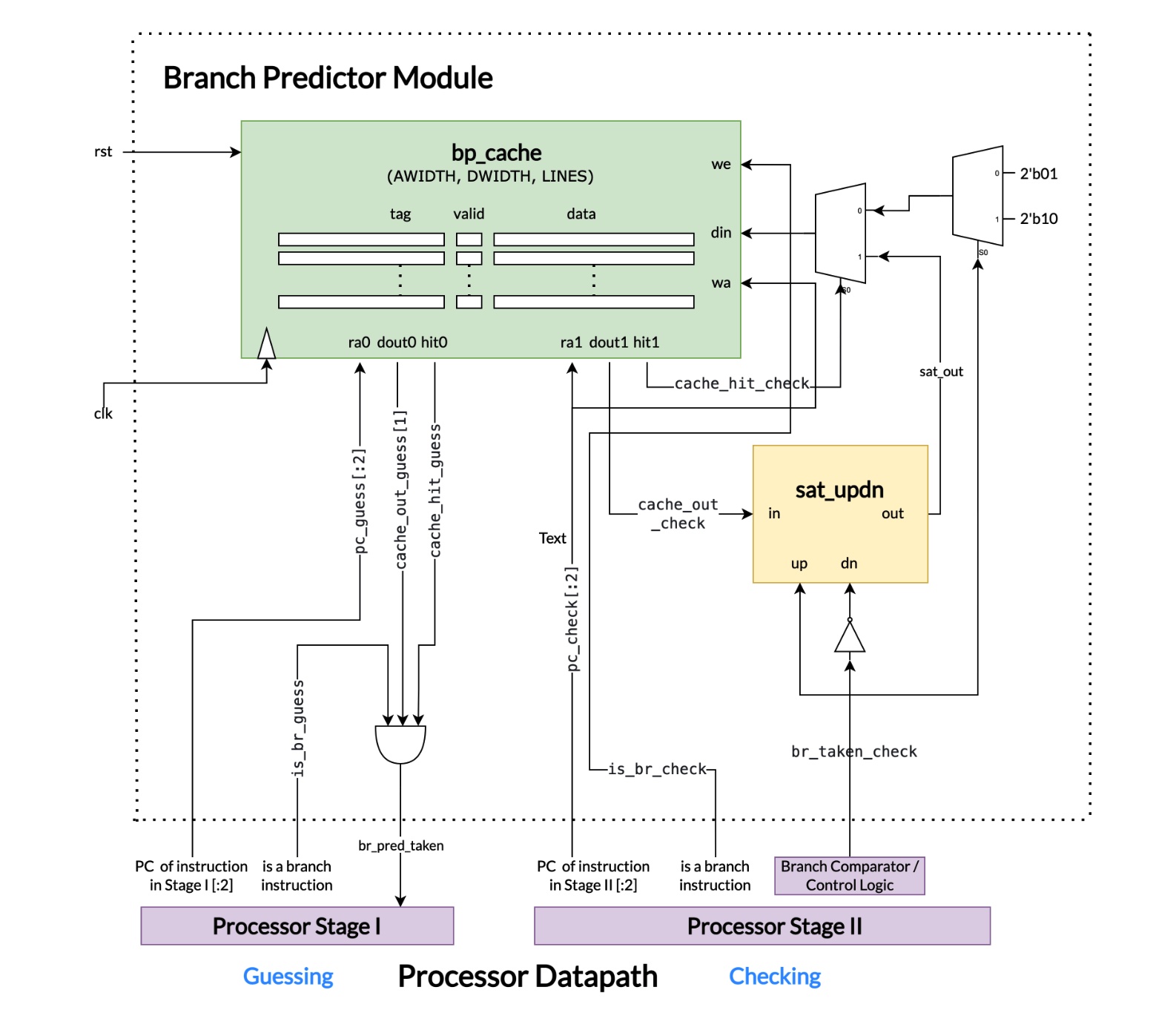
It is able to:
- Guess: When the branch instruction is in the first stage of processor, make a prediction whether to take the branch based on the past history
- Check: When the branch instruction reaches the second stage of processor (where branch result is resolved), check if the prediction is correct and update to make a better prediction next time
Optimization
We were able to get our CPU running at a clock frequency of 105MHz by reducing the critical path of the Execute stage; our base design initally only supported 60MHz.
The following reports are testing done with a benchmark mmult program during various stages of optimization. The instruction count for all of these runs is 12,894,955 (since we are running the same program each time).
| Change | Maximum Clock Frequency (MHz) | Cycle Count | CPI | Utilization | Time (μs) |
|---|---|---|---|---|---|
| Base | 60 | 13,949,613 | 1.0818 | 1831 LUTs, 34 Block RAMs, 671 FFs, 0 Latches, 0 DSPs | 232,494 |
| Eliminate M-X forwarding and replace with data stalls in X | 80 | 14,736,115 | 1.1428 | 1656 LUTs, 34 Block RAMs, 680 FFs, 32 Latches, 0 DSPs | 184,201 |
| Moved stalls to F stage | 90 | 14,736,115 | 1.1428 | 1586 LUTs, 34 Block RAMs, 665 FFs, 32 Latches, 0 DSPs | 162,725 |
| Precompute memory inputs during F stage | 105 | 14,736,115 | 1.1428 | 1756 LUTs, 34 Block RAMs, 754 FFs, 32 Latches, 0 DSPs | 140,343 |